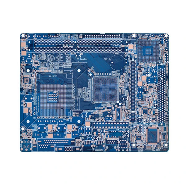
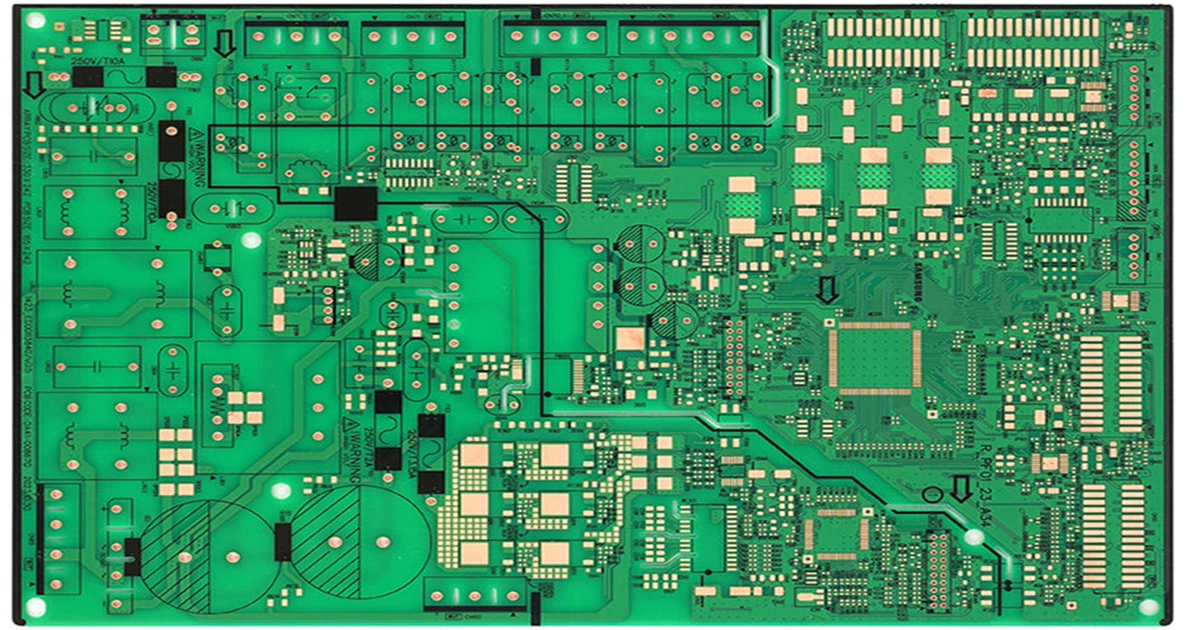
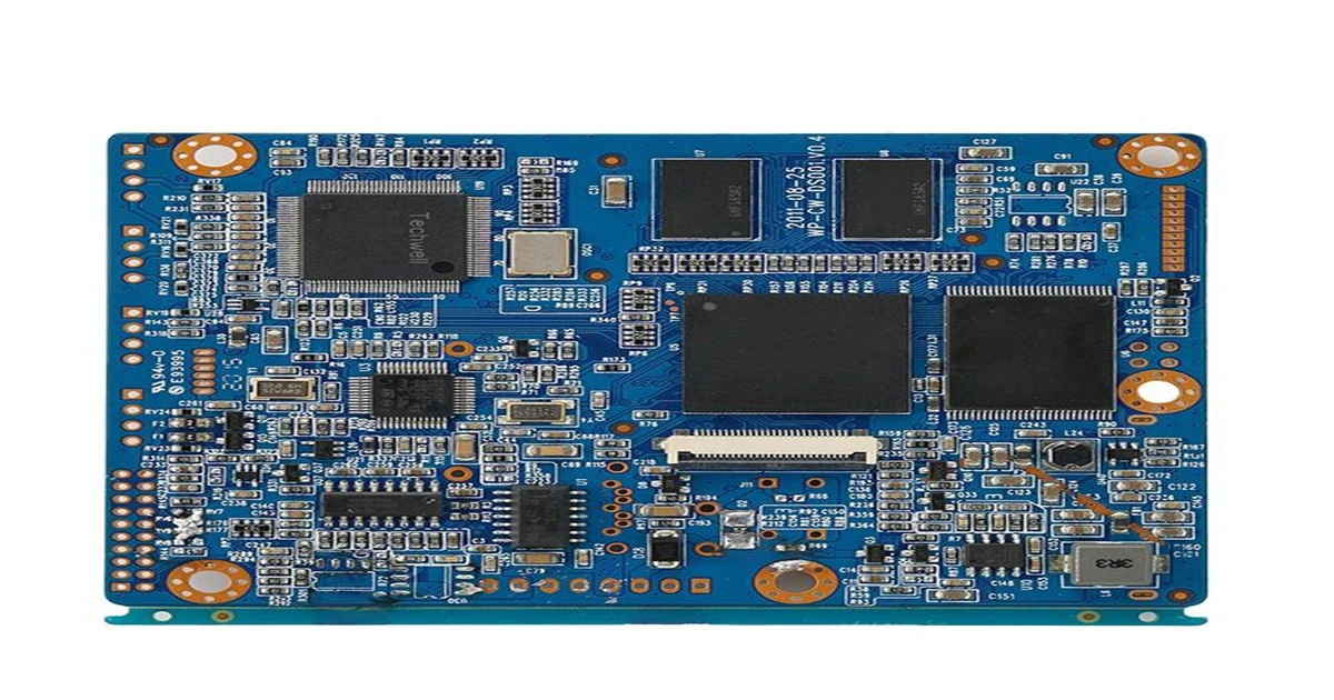
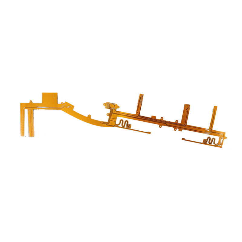
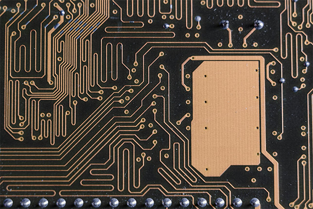
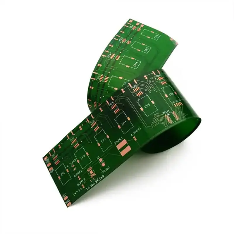
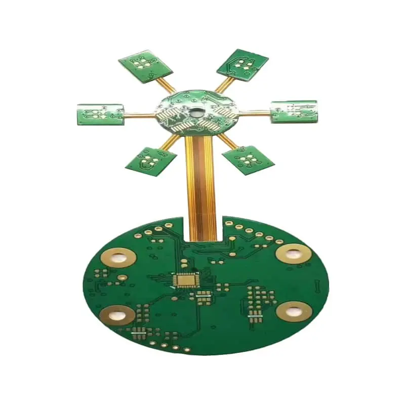
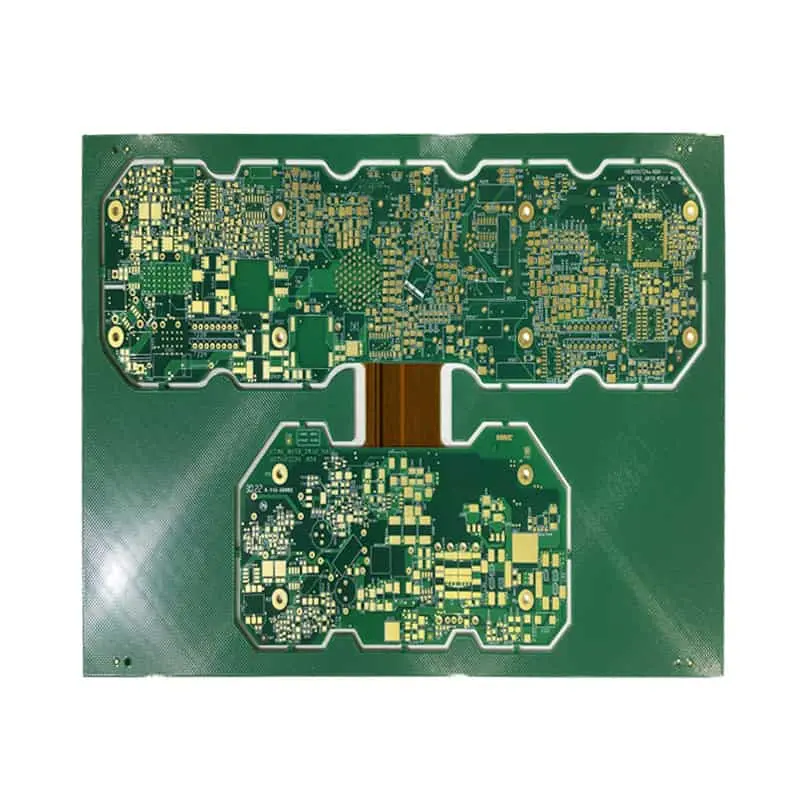
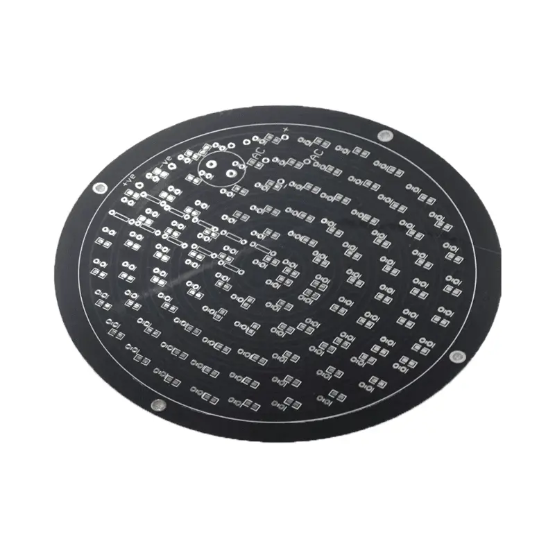
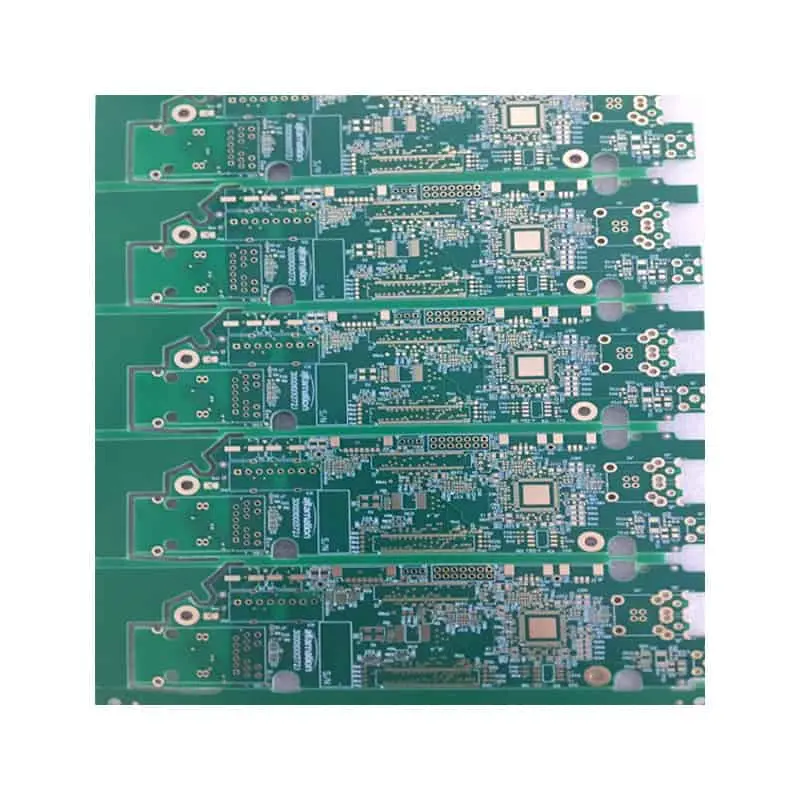
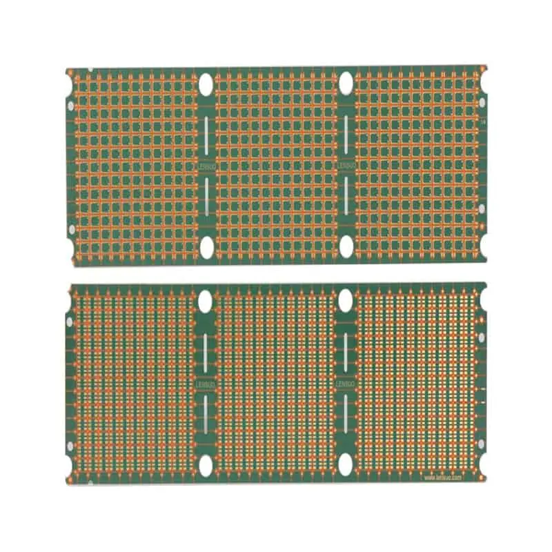
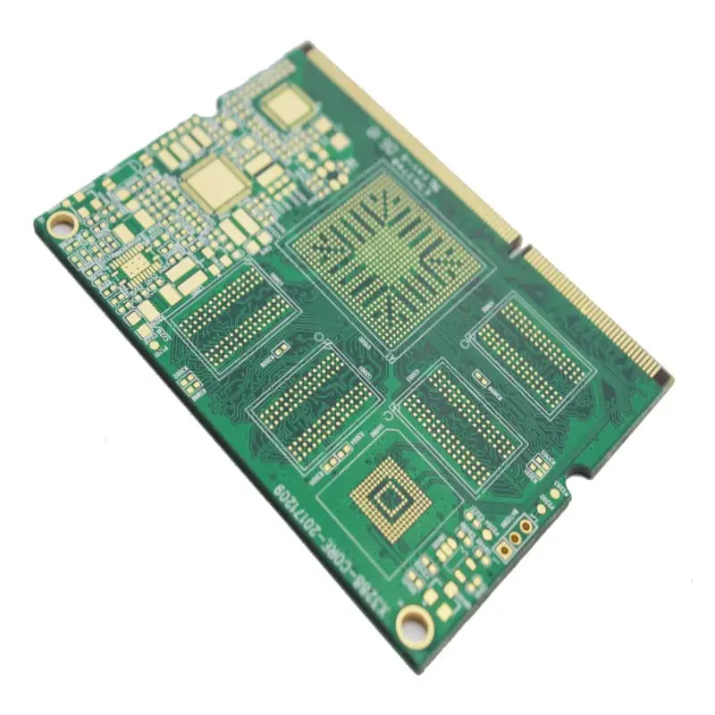
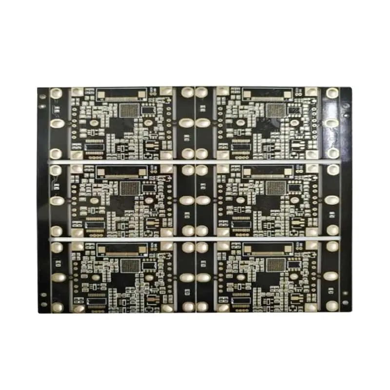
A copper core PCB (Printed Circuit Board) is a key component in modern electronics, valued for its superior thermal management and mechanical stability. This guide outlines the essentials of copper core PCBs, their manufacturing process, and the reasons for their use.
What is a Copper Core PCB?
A copper core PCB features a central layer of copper, providing excellent thermal conductivity crucial for high-power electronic applications. The typical structure includes:
– Top copper layer
– Dielectric layer
– Copper core
– Dielectric layer
– Bottom copper layer
The copper core’s thickness varies depending on the application, commonly ranging from 1.0 mm to 3.0 mm.
Manufacturing Process of Copper Core PCB
The manufacturing process of a copper core PCB involves several critical steps, each contributing to the board’s final quality and performance.
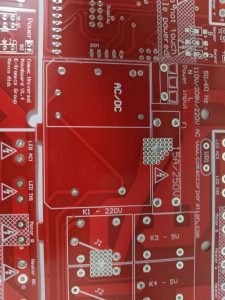 Step 1: Design and Material Selection
The process starts by designing the PCB layout using CAD software. During this phase, both electrical and thermal requirements are considered to determine the optimal thickness of the copper core and the dielectric layers. High-quality materials, such as polyimide or FR4, are selected for the dielectric layers to ensure reliability and performance.
Step 2: Lamination
Lamination involves layering the materials together under high pressure and temperature. The copper core is sandwiched between dielectric layers, and copper foil is added to the top and bottom surfaces. The typical lamination conditions include a temperature of 180-220°C and a pressure of 200-400 psi, with a curing time of approximately 1-2 hours. This step is crucial for ensuring the structural integrity of the PCB.
Step 3: Drilling and Plating
After lamination, holes are drilled into the PCB to create vias, which allow electrical connections between the layers. The drilled holes are then plated with copper to create conductive paths. The copper plating process involves immersing the PCB in a copper sulfate solution and applying an electric current, resulting in a copper deposit with a thickness of 25-50 micrometers. This step ensures robust electrical connections.
Step 4: Imaging and Etching
In this step, the PCB is coated with a photoresist and exposed to ultraviolet light through a photomask, which defines the circuit pattern. The exposed areas of the photoresist harden, while the unexposed areas remain soft and wash away. The PCB is then immersed in an etching solution, such as ferric chloride, to remove the unwanted copper, leaving behind the desired circuit pattern.
Step 5: Solder Mask and Surface Finish
Apply a solder mask to the PCB to protect the copper wires and prevent short circuits during soldering. The solder mask is typically green but can be other colors as well. Finally, a surface finish, such as HASL (Hot Air Solder Leveling) or ENIG (Electroless Nickel Immersion Gold), is applied to the exposed copper pads. This step enhances solderability and protects against oxidation, ensuring the longevity and reliability of the PCB.
Why Use Copper Core in PCB?
There are several advantages to using a copper core in PCB manufacturing:
– Thermal Management: Copper core PCBs excel in dissipating heat, which is essential for high-power applications such as LED lighting, automotive electronics, and power supplies.
– Mechanical Stability: The copper core provides structural integrity, reduces the risk of warping, and increases PCB durability.
– Electrical Performance: Copper’s excellent conductivity ensures minimal signal loss and improved electrical performance, which is critical for high-frequency applications.
Conclusion
The copper core PCB is a pivotal innovation in electronics, offering superior thermal management, mechanical stability, and electrical performance. By understanding the materials used, the manufacturing process, and the benefits of using a copper core, manufacturers can produce high-quality PCBs that meet the stringent requirements of modern electronic applications. From design to final surface finish, each step in the manufacturing process is crucial to achieving the desired performance and reliability of the copper core PCB.
