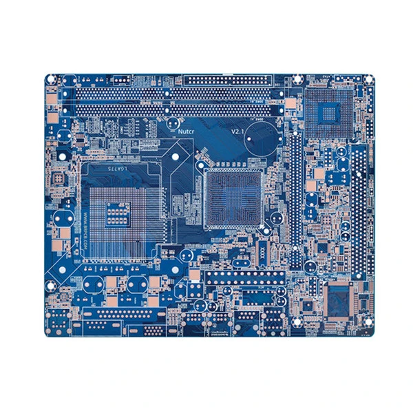
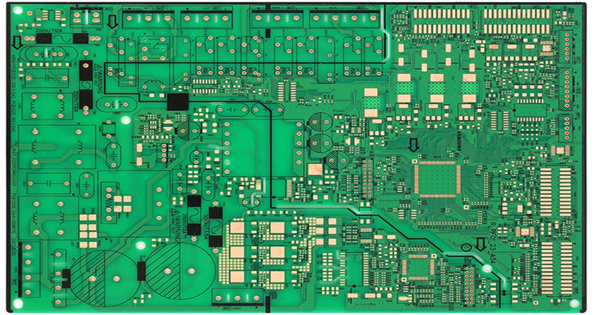
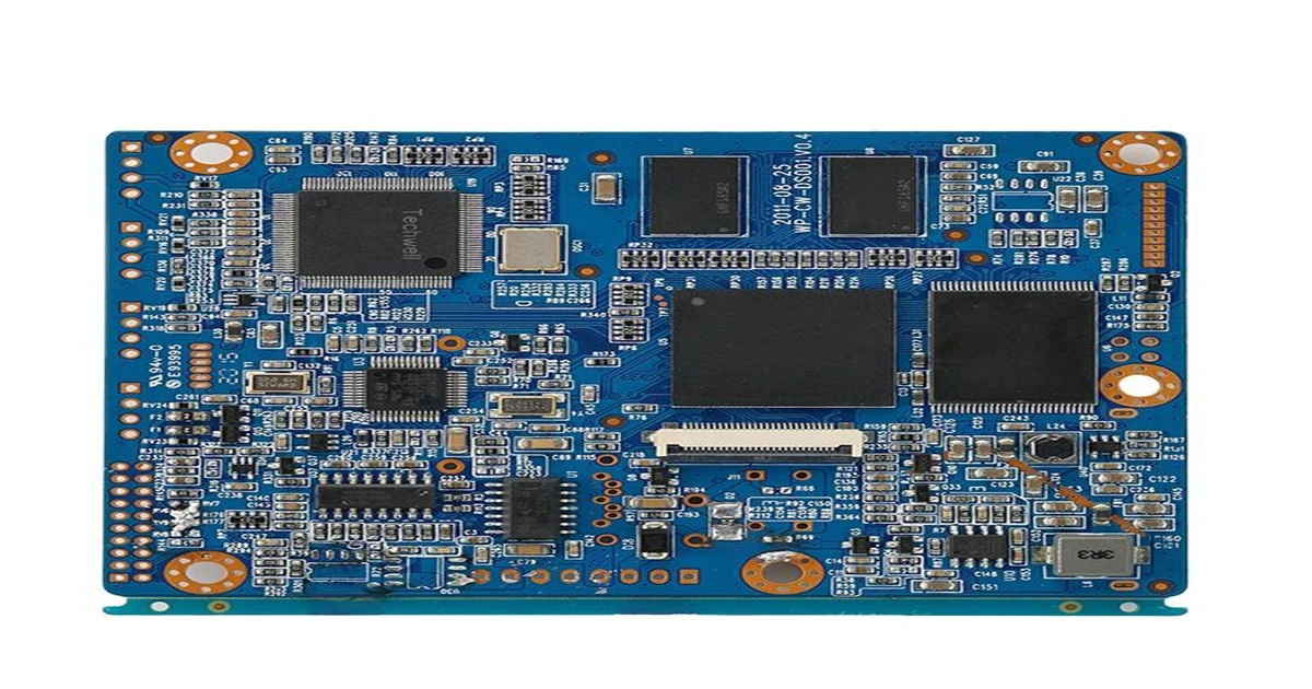
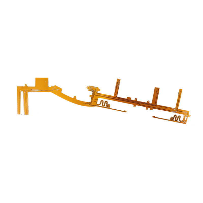
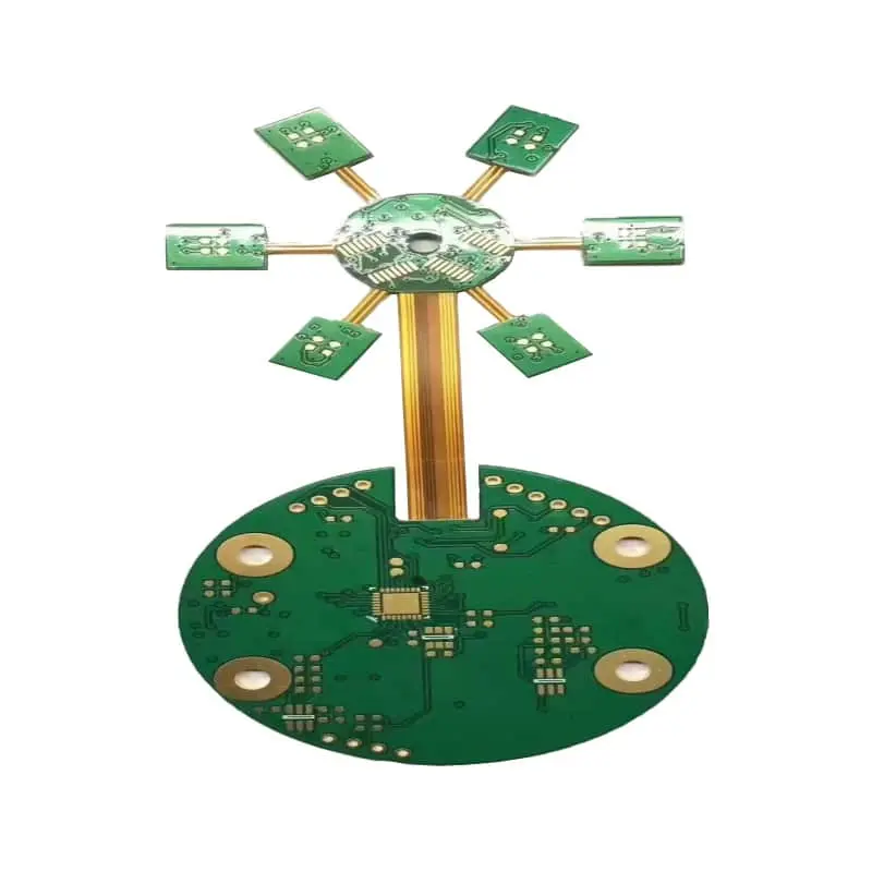
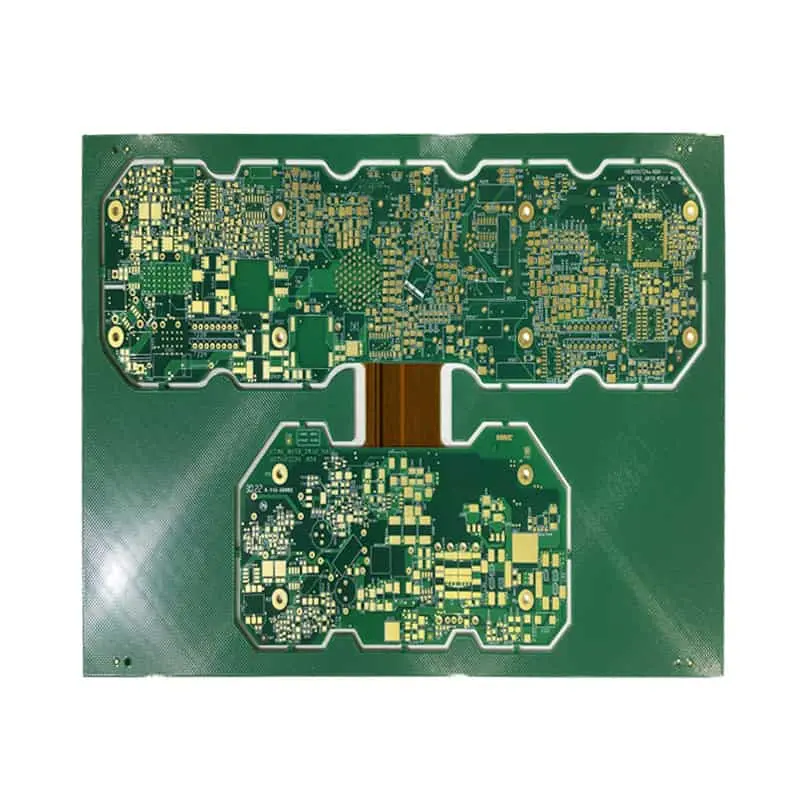
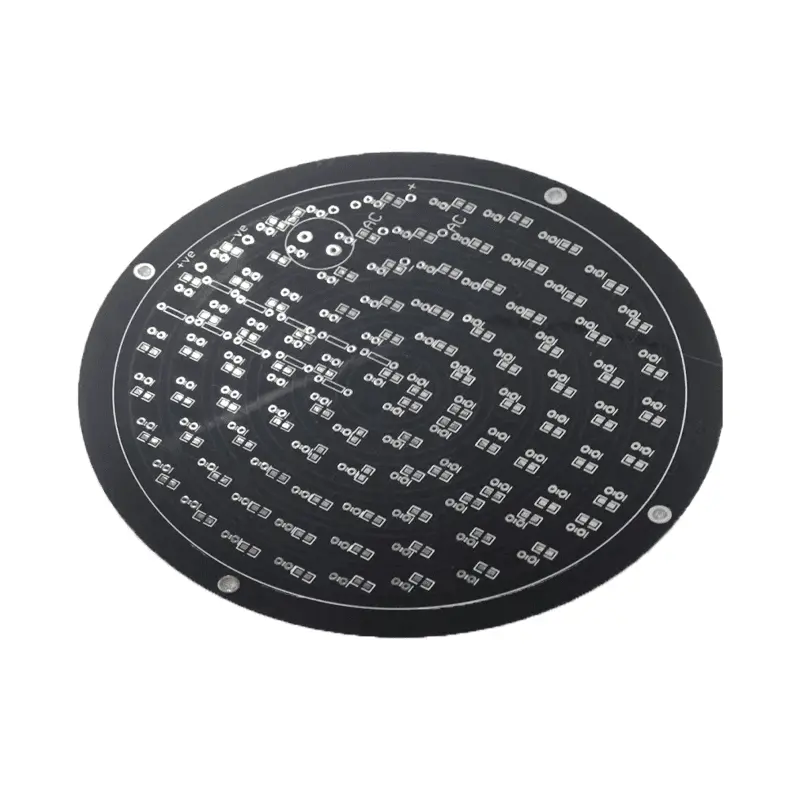
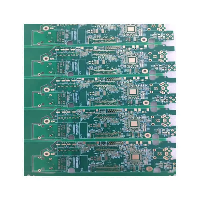
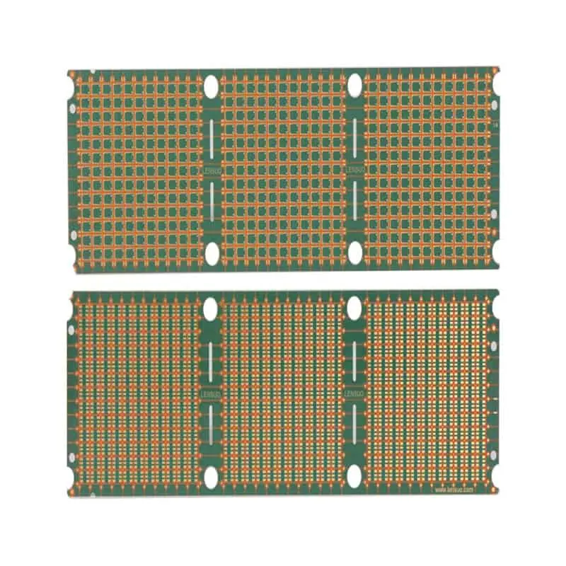
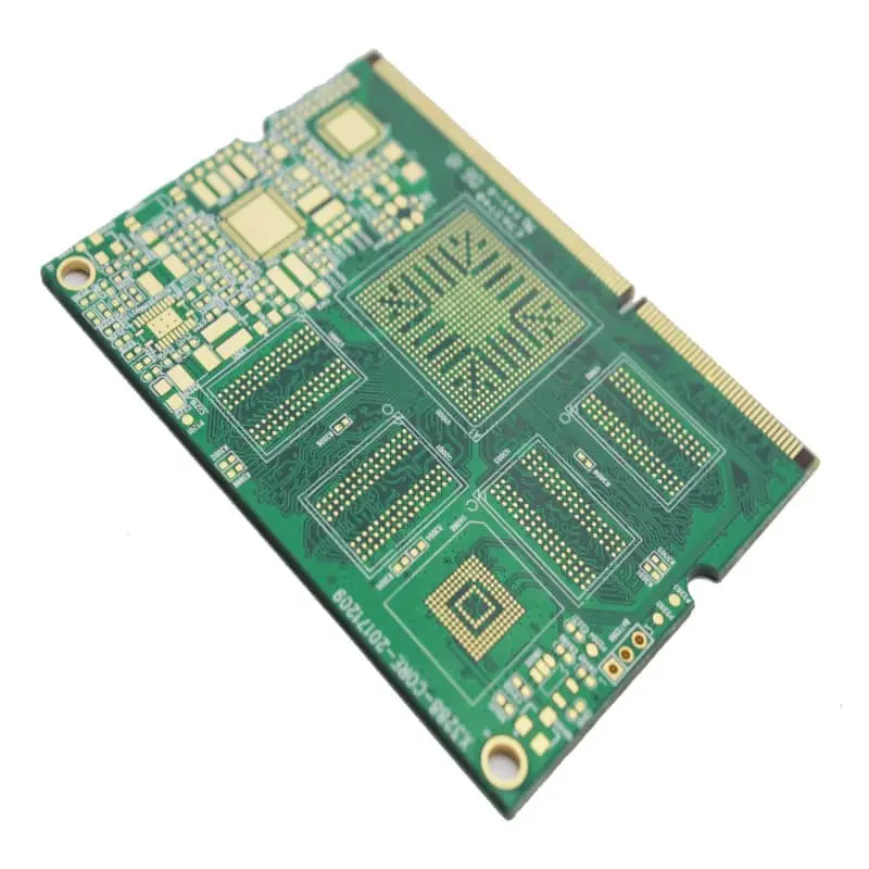
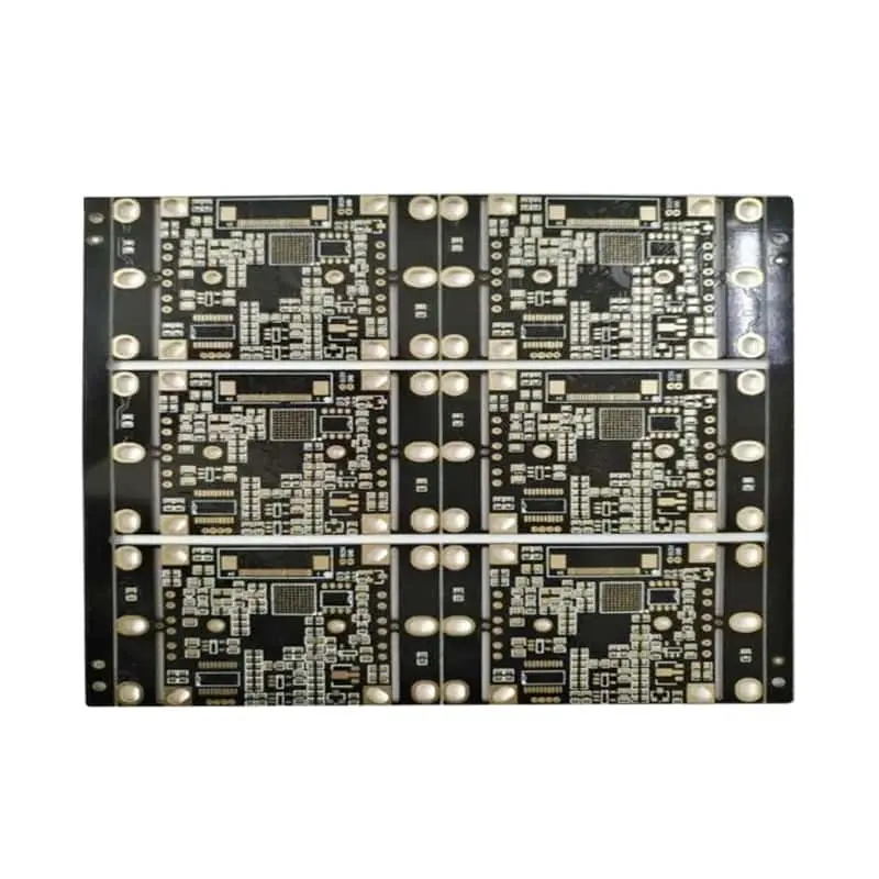
Multilayer printed circuit boards (PCBs) are crucial in the world of electronics, facilitating complex circuitry within a compact design. This article will explore what a multilayer printed circuit board is, compare it with single-layer PCBs, and outline the detailed manufacturing process involved in creating these sophisticated components.
What Is a Multilayer Printed Circuit Board?
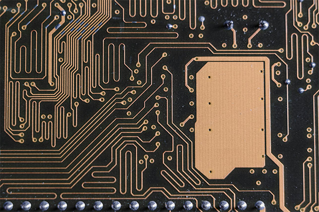
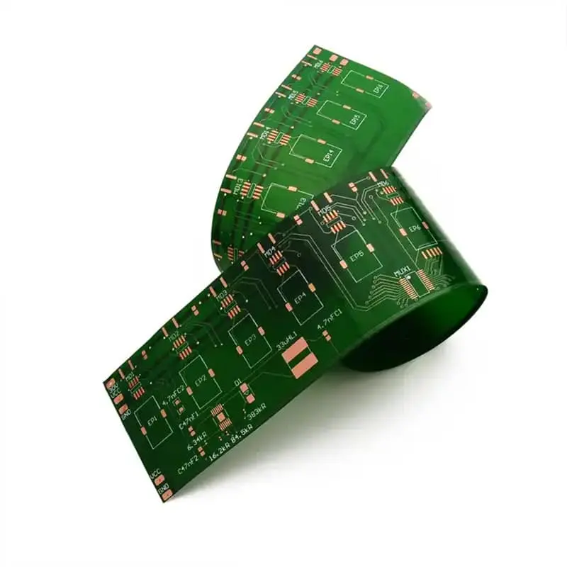
A multilayer printed circuit board is composed of three or more layers of conductive pathways, allowing for complex electronic circuits to be densely packed into a small footprint. Each layer is separated by insulating material, usually made of fiberglass epoxy, which provides mechanical strength and electrical insulation. This multilayer structure is essential for advanced electronic devices, including smartphones, computers, and medical equipment, where space and performance are critical.
Comparing Single-Layer and Multilayer PCBs
Single-layer PCBs consist of one layer of conductive material, making them simpler and less expensive to manufacture. They are typically used in basic electronic applications where circuit complexity is low. In contrast, multilayer printed circuit boards offer several advantages:
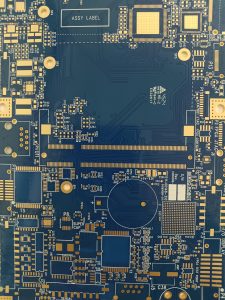 Density: Multilayer PCBs can house more components, which is essential for compact devices.
Performance: With multiple layers, designers can optimize signal integrity and reduce electromagnetic interference.
Versatility: They can accommodate complex routing and higher power applications, making them suitable for a wide range of industries.
While single-layer PCBs are sufficient for simple tasks, multilayer printed circuit boards are indispensable for modern electronics.
Steps in Manufacturing a Multilayer Printed Circuit Board
The manufacturing process of a multilayer printed circuit board involves several intricate steps:
- Design Phase: The process begins with creating a detailed schematic using Computer-Aided Design (CAD) software. Engineers outline the circuit paths and determine the number of layers required. A typical multilayer PCB may have 4 to 12 layers, depending on complexity.
- Material Selection: High-quality materials are essential for a multilayer printed circuit board. The substrate is usually fiberglass epoxy, and copper foil is selected based on the desired conductivity and thickness, typically ranging from 0.5 to 3 ounces per square foot.
- Layer Preparation: Each layer is cut to size and coated with a layer of copper. The thickness of the copper layer is critical, as it affects current carrying capacity and heat dissipation.
- Lamination: The prepared layers are stacked with prepreg material, which acts as a bonding agent. This assembly is placed in a hydraulic press at around 300°F (149°C) and 300 psi (2.07 MPa) for approximately 60 minutes. This process cures the prepreg and firmly bonds the layers together.
- Drilling Vias: Once laminated, precision holes are drilled into the multilayer printed circuit board to create vias. These vias enable electrical connections between layers. Advanced laser drilling can achieve hole sizes as small as 0.1 mm, ensuring minimal space usage.
- Copper Plating: The drilled vias are plated with copper to establish interconnections between layers. The plating thickness is typically around 1–2 mils (0.025–0.05 mm), ensuring robust connectivity.
- Etching: After plating, a photoresist layer is applied to the board, and the desired circuit pattern is exposed using ultraviolet light. The exposed areas are developed and etched away with a chemical solution, leaving the desired copper traces.
- Final Finishing: The multilayer printed circuit board undergoes surface finishing, which may include applying a solder mask to protect the circuitry. A silkscreen layer is added for component labeling, enhancing usability.
- Testing and Quality Control: Rigorous testing is performed to ensure the board meets electrical and mechanical standards. This may include automated optical inspection (AOI) and electrical testing to verify connectivity and functionality.
Conclusion
The creation of a multilayer printed circuit board is a complex process that combines advanced technology with precise engineering. Understanding how a multilayer printed circuit board is made—from design and material selection to lamination and testing—highlights the sophistication behind modern electronics. As technology continues to advance, the capabilities of multilayer PCBs will expand, driving innovation in various industries and paving the way for future electronic developments. If you want to know more or have a demand for multilayer printed circuit boards, please browse PCBCOMING’s catalog.
