 1. Material Selection: The Backbone of High-Frequency Performance
The choice of materials significantly impacts the performance of high-frequency PCBs. Key materials include:
FR4 Base Material: A widely used substrate for PCBs, known for its excellent electrical and thermal properties. Its high dielectric constant makes it ideal for maintaining signal integrity at high frequencies.
Polyester Substrates: These materials, including polyimides, are popular for high-frequency applications due to their low loss tangent and good mechanical durability.
Customized Substrates: For specialized applications, substrates tailored to specific frequency ranges and impedance requirements are developed.
Selecting the right material ensures that the PCB can handle the demanding conditions of high-frequency operation without signal degradation or thermal issues.
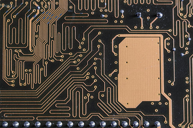
2. Microwave-Level Design: Layout and Structure
High-frequency PCBs often require microwave-level design considerations, which include:
Multi-Layer Structures: High-frequency signals can become unstable in single-layer PCBs, necessitating the use of multi-layer structures to accommodate multiple signal layers and ground planes.
Through-Signal Layers: These layers allow for direct routing of signals over long distances, reducing parasitic inductance and capacitance (L, C) that can distort high-frequency signals.
Terminations and Coupling: Proper terminations and minimized signal coupling are crucial to maintain signal integrity and prevent interference between traces.
Impedance Matching: Ensuring that the impedance of the traces matches the impedance of the connected components is vital for reducing reflections and power loss.
3. Signal Integrity Management: Frequencies and Noise
Maintaining signal integrity at high frequencies is a challenge due to increased susceptibility to noise and interference. Key strategies include:
Optimized Layout: By minimizing signal crosstalk and reducing the proximity of traces to ground planes, the overall noise level can be controlled.
Minimized Parasitic Effects: Techniques such as careful routing and the use of guard traces help reduce the parasitic inductance and capacitance that can degrade signal quality.
Low-Density laminates: High-frequency applications often benefit from low-density PCBs, which have fewer dielectric losses and are more amenable to high-speed signal transmission.
4. Advanced Manufacturing Techniques
The manufacturing process of high-frequency PCBs demands advanced techniques to ensure precision and reliability:
Surface Mount Technology (SMT): SMT reduces soldering time and increases PCB density, making it ideal for high-frequency applications.
Drill-and-Weld (TS) Technology: This technique allows for precise through-hole and surface-mount components, ensuring minimal signal degradation.
No Lead Production (UL): Adhering to environmental and regulatory standards, UL-free manufacturing reduces potential hazardous residues, enhancing product safety.
5. Testing and Validation
Thorough testing is essential to validate the performance of high-frequency PCBs:
Network Analyzers: These instruments measure S-parameters, impedance, and crosstalk to assess signal integrity and overall system performance.
Multimeter Measurements: Conducting DC and AC measurements ensures that voltage levels and power dissipation are within acceptable limits.
EMI/ESD Testing: High-frequency PCBs are subjected to electromagnetic interference (EMI) and electrostatic discharge (ESD) testing to ensure robustness in real-world conditions.