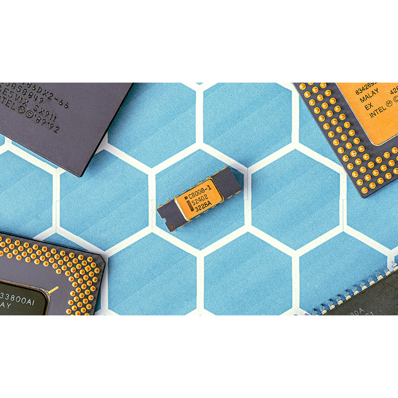
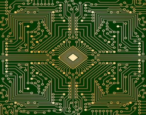
In today’s high-speed, miniaturized electronics landscape, High-Density Interconnect (HDI) PCBs are the backbone of innovation. At PCBCOMING, we combine cutting-edge manufacturing technologies with decades of expertise to deliver HDI PCBs that redefine reliability, precision, and performance.
Why Our HDI PCBs Stand Out
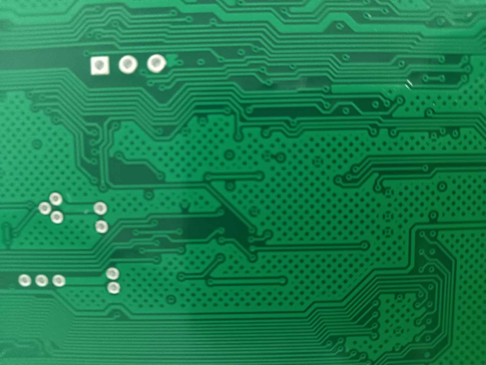
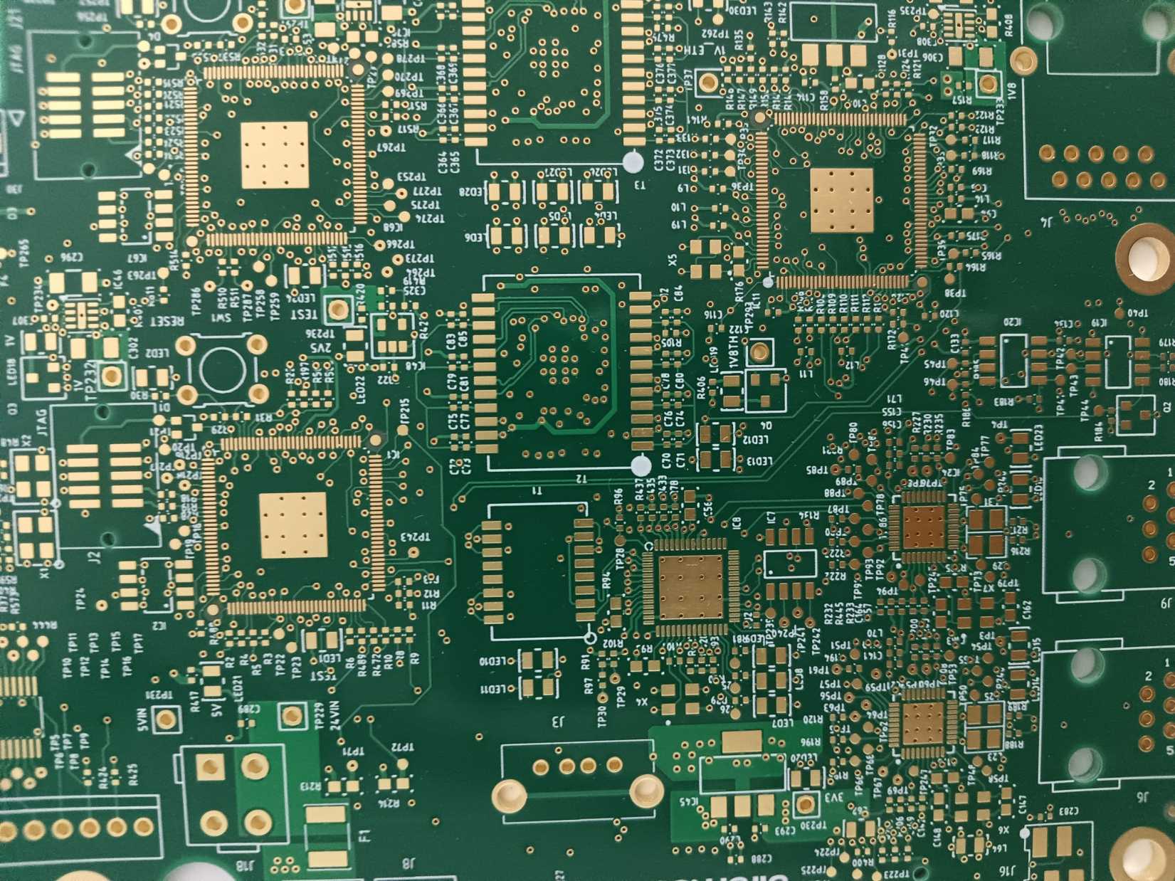
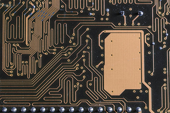
1. Sub-2μm Line/Space & AnyLayer® Microvia Technology
Achieve 2/2μm trace/space resolution with Laser Direct Imaging (LDI) and modified Semi-Additive Process (mSAP).
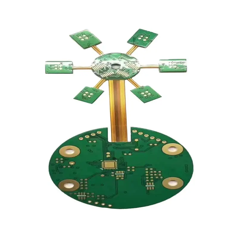
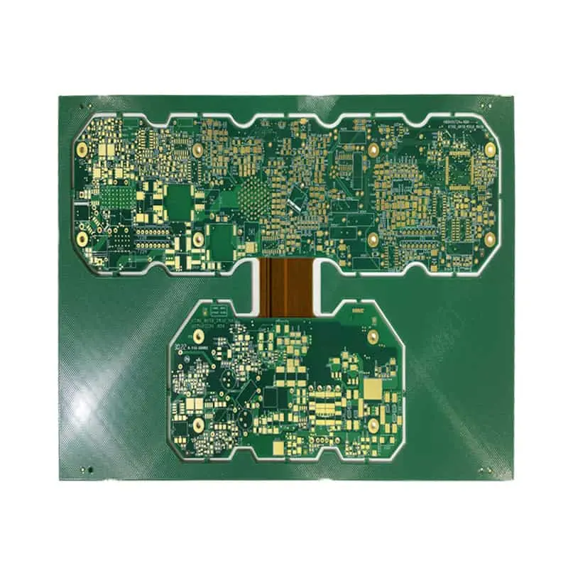
AnyLayer® stacked microvias (CO₂ + UV laser drilling) enable 20+ layer counts in 0.4mm thickness for ultra-compact designs.
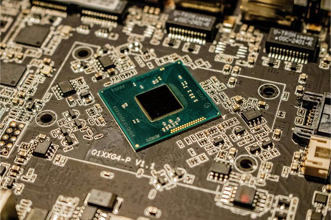
2. High-Frequency & Thermal Mastery
±3% impedance control up to 40GHz using low-loss materials (MEGTRON 7, Rogers 4350B).
Embedded passive components (resistors, capacitors) reduce signal loss and board size by 30%.
3. Reliability Engineered for Critical Applications
1000+ thermal cycles (-55°C to 150°C) with <5% expansion rate (high-Tg FR4/Polyimide).
99.99% via reliability tested under IPC-6012 Class 3/AEC-Q200 standards.
Applications Redefined
5G & AI Infrastructure: 0.2mm pitch BGA routing for mmWave antennas and AI accelerators.
Automotive Electronics: AEC-Q100-qualified HDI boards for ADAS, LiDAR, and EV battery management.
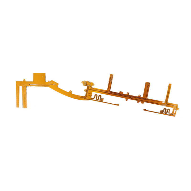
Medical Implants: Biocompatible, 0.1mm flexible HDI for pacemakers and wearable diagnostics.
Aerospace & Defense: MIL-PRF-31032 compliant boards with EMI shielding for harsh environments.
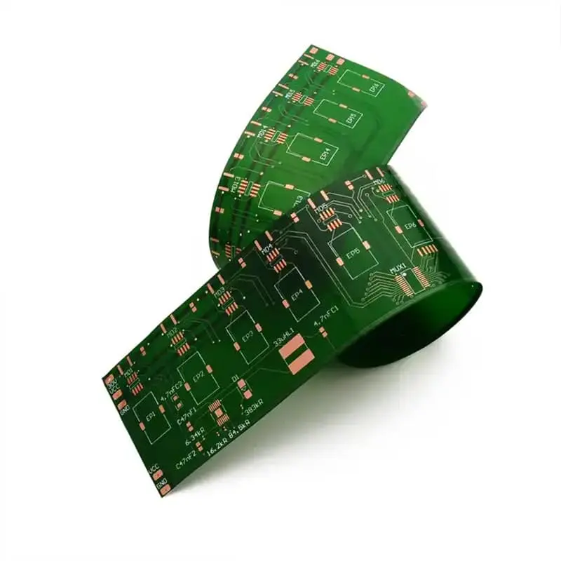
Consumer Tech: Foldable smartphone HDI rigid-flex hybrids with 500K+ dynamic bend cycles.
Certified Quality, Global Trust
IATF 16949 (automotive), ISO 13485 (medical), and AS9100D (aerospace) certified.
100% AOI/3D X-ray inspection and real-time yield analytics via IoT-enabled production lines.
UL 94 V-0 flame-retardant and RoHS/REACH-compliant material options.
Speed Meets Precision
5-day prototypes for complex HDI designs (blind/buried vias, via-in-pad).
30-day mass production with https://www.pcbcoming.com/