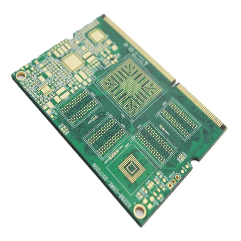
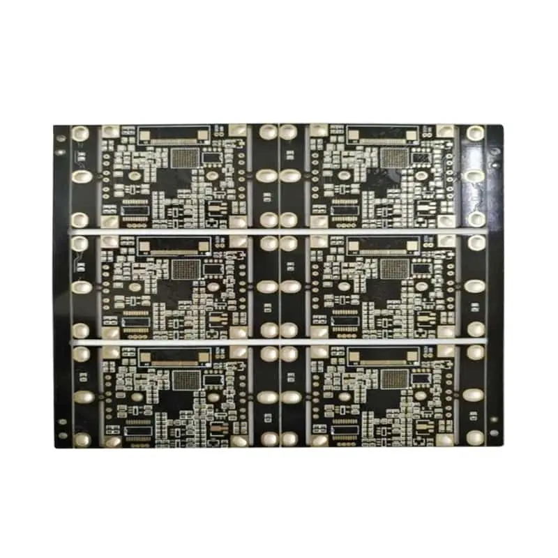
Blind and buried vias are essential components in modern multilayer printed circuit boards (PCBs). These specialized vias increase the functionality and density of PCBs, making them an integral part of high-performance electronic products. Understanding their structure, manufacturing processes, and applications helps engineers optimize designs for advanced technology.
Definition of Blind and Buried Vias
What Are Blind Vias?
Blind vias connect an outer layer of a PCB to one or more inner layers without passing through the entire board. This configuration saves space on the surface while maintaining layer-to-layer connectivity. Blind vias are common in compact devices like smartphones and wearable electronics, where space constraints are critical.
What Are Buried Vias?
Buried vias, unlike blind vias, are completely enclosed within the PCB. They connect two or more inner layers, remaining invisible from the surface. This type of via is crucial in complex PCBs where routing density and signal integrity are top priorities.
How to Manufacture Blind and Buried Vias
The manufacturing process for blind and buried vias involves precision drilling and plating. The two primary techniques are:
 Laser Drilling
Laser drilling creates holes with diameters as small as 0.1 mm, ideal for high-density interconnect (HDI) PCBs. The laser ensures accuracy and minimal damage to surrounding layers, making it a preferred method for blind vias.
Mechanical Drilling
For larger vias, mechanical drilling is used. Advanced CNC machines can drill with tolerances as tight as ±0.02 mm. After drilling, copper plating ensures electrical conductivity.
Sequential Lamination
Sequential lamination is necessary for buried vias. Inner layers are drilled and plated first, then laminated with other layers. This step-by-step process ensures buried vias are correctly aligned and connected.
Applications of Blind and Buried Vias
High-Density Interconnect PCBs
Blind and buried vias are integral to HDI PCBs, enabling denser routing and smaller form factors. For instance, a 10-layer HDI PCB can accommodate blind vias with depths of 0.3–0.5 mm, providing connectivity without compromising board integrity.
Multilayer PCBs in Automotive and Aerospace
Automotive and aerospace industries rely on multilayer PCBs with blind and buried vias for advanced navigation and control systems. These vias reduce signal loss and improve reliability in harsh environments.
Consumer Electronics
Devices like smartphones utilize blind vias to maximize board real estate, allowing more components to fit in smaller spaces. Buried vias enhance signal performance by isolating critical pathways within the PCB.
Advantages and Design Considerations
Advantages
- Space Efficiency: Blind and buried vias save surface area, enabling smaller devices.
- Improved Signal Integrity: Reducing via lengths minimizes signal interference.
- Layer Connectivity: These vias allow intricate designs in multilayer PCBs.
Design Considerations
Designers must account for manufacturing constraints and costs. For example, including multiple blind vias increases complexity and price. Simulations help ensure designs meet performance criteria without unnecessary layers.
Conclusion
Blind and buried vias are foundational to modern electronics, offering space-saving solutions and enhancing performance. From HDI PCBs to aerospace applications, their precise manufacturing and versatility make them indispensable. Understanding what blind and buried vias are, how they are made, and their practical uses empowers engineers to push the boundaries of PCB design.
